

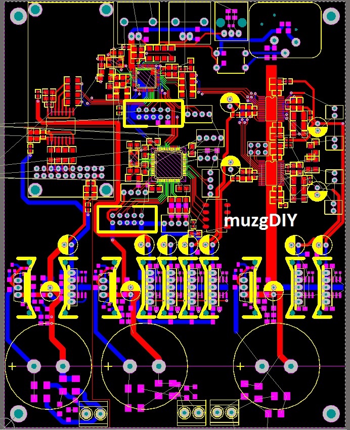
In addition to new preamplifier module I would like to present dedicated power supply. This simple module have both anode and heater rails regulated and stabilised. Anode regulator is based on discrete components.
Dimensions: 100 x 60 mm
Uncompromising quality at an affordable price
In addition to new preamplifier module I would like to present dedicated power supply. This simple module have both anode and heater rails regulated and stabilised. Anode regulator is based on discrete components.
Dimensions: 100 x 60 mm
This power supply is complete solution for tube pre- and amplifiers – simple and complex as well. It is based on semiconductors and contains both: anode and heater stabilised power supply.

Maybe you will be surprised, but most of this unit is made of SMD components. Only some critical parts are THT – power, and capacitors.

Circuit is designed to meet even most extreme requirements. Could be used to power simple single tube preamplifier and extreme balanced tube preamplifier with differential amplifier and 4x White Cathode followers created with 6N30P tubes. In addition, it is possible to power small amplifiers for example: stereo EL84 SE Amp, or single channel EL84 PP Amp.

Single PCB contains:
Anode power supply is built over discrete high voltage regulator similar to my V3.1 regulators. This means that this regulator is completely discrete, based upon SMD components, specially selected to operate with voltages up to 400V. Output voltage is set by potentiometer or could be set by fixed resistor.
Anode regulator is preceded by CRC smoothing filter for best noise performance and also to increase overall PSRR.
Heater power supply is based on integrated LDO and is capable to deliver up to 5A. Voltage at its output rises slowly from 1,2V to desired voltage in 10s to protect tube heaters from current surge when they are cool. Output voltage selection can be done in 2 ways:

Bridge rectifier in this circuit is created from 10A Schottky diodes to provide low voltage drop at the input. All this circuit is preceded with CLC smoothing circuit for best noise performance.
Heater supplying voltage is balanced and elevated comparing to anode supply GND by 1/4 of anode voltage. This feature is helpful in circuit when cathodes of tubes are biased by high voltage for example: SRPP, White Cathode Followers, Mu Followers.
The last part of the board is control unit. This circuit contains two part: anode delay circuit and audio muting circuit. Timing is set to 30s delay of anode voltage and 40s for audio mute. Timers as well as relay output are powered by third, 5V regulator. Thanks to this initial delay it is stable in every condition and relay is always powered from stable voltage.

Best thermal performance is achieved by good thermal design. This supply is able to dissipate a lot of power.
And in addition all this things were achieved in dimensions: 100 x 100 x 50mm!!
Enjoy. 😉
I start a topic concerning my new project that is DAC based on PCM1794A chips. On chips because it may be built either on two or one PCM1794 chip what is configurated by appropiate set of elements (more details on schematic).
Schematics: PCM1794_DIX9211_DAC_V10
As a S/PDIF receiver and I2S switch I used relatively not well known DIX9211 chip. Its main advantages are twelve S/PDIF inputs, support for all formats ranging till 192kHz, a possibility of connecting to three additional 12S signal sources (it may also allow DSD format) and controlling via I2C. DAC also has a space for amanero module with its own power supply and galvanic isolation ISO7640.
Module’s inputs are:
DAC is controlled by microcontroller STM32F100RBT6B. STM32F100RBT6B has big amount of periphery that allow to expanse DAC, a lot of GPIO and 128kB of flash memory and that all is well-priced. Additional simplification which is Cube makes there is no other choice. Encoder was planned to be responsible for controlling. Active input indication via separate PCB with OLED on SPI display or 8 LEDs on 74HC595. There is possibility to control via remote control or UART. Updates are made via UART. To PCB programming ST-Link V2 is needed. It is available on each Discovery STM32 module.
Power supplying is extended. I divide it on three sections, each supplied from separate transformer winding.
Each section is built in similar way:
Rectifier -> big snap capacitor -> discrete pre-regulator (V1.2) -> post-regulator
Post- regulators may be chosen between LT1763 and discrete module. Additionally, I put LC filters in digital sections. Thanks to that they are better separated. Digital module contain 10 voltage regulators. In MONO mode (one PCM1794 for canal?) there is possibility to supply the chip from different regulators (4pcs,) or mounting jumper and using only two – one for digital and one for analogue.
The whole construction I divide on two different modules – digital PCB with DAC chips (150x120mm) and totally symmetrical analogue module with the same dimensions (not ready yet). Such division make it elegant and not as big as a computer board, and what matters more it leave a space to experiment with other analogue variants, also with lamps.
I plan to build analogue module as follow:
Later I will work out lamp module.
The whole circuit, where it possible, in SMD. The elements dimensions from 0603 to 1210. PCB is still being worked out. I attach the look/view.
Big success of V3.1 regulator shows me that this topology has a huge potential to implement in many applications. For those who uses my V3.1 regulator to create its standalone power supply I have got something interesting! V2.0 power supply which is better and stronger implementation of V3.1 topology.
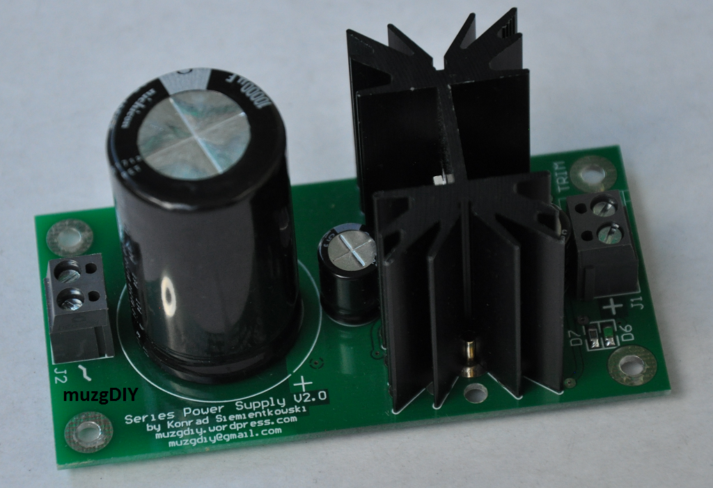
Better means 3 more current sources which replace resistors. This give us better PSRR, more gain in error amplifier and better immunity to output current ripple.
Stronger means that is equipped with powerful TO220 transistor on dedicated heatsink. This gives me possibility to increase output current up to 3A!
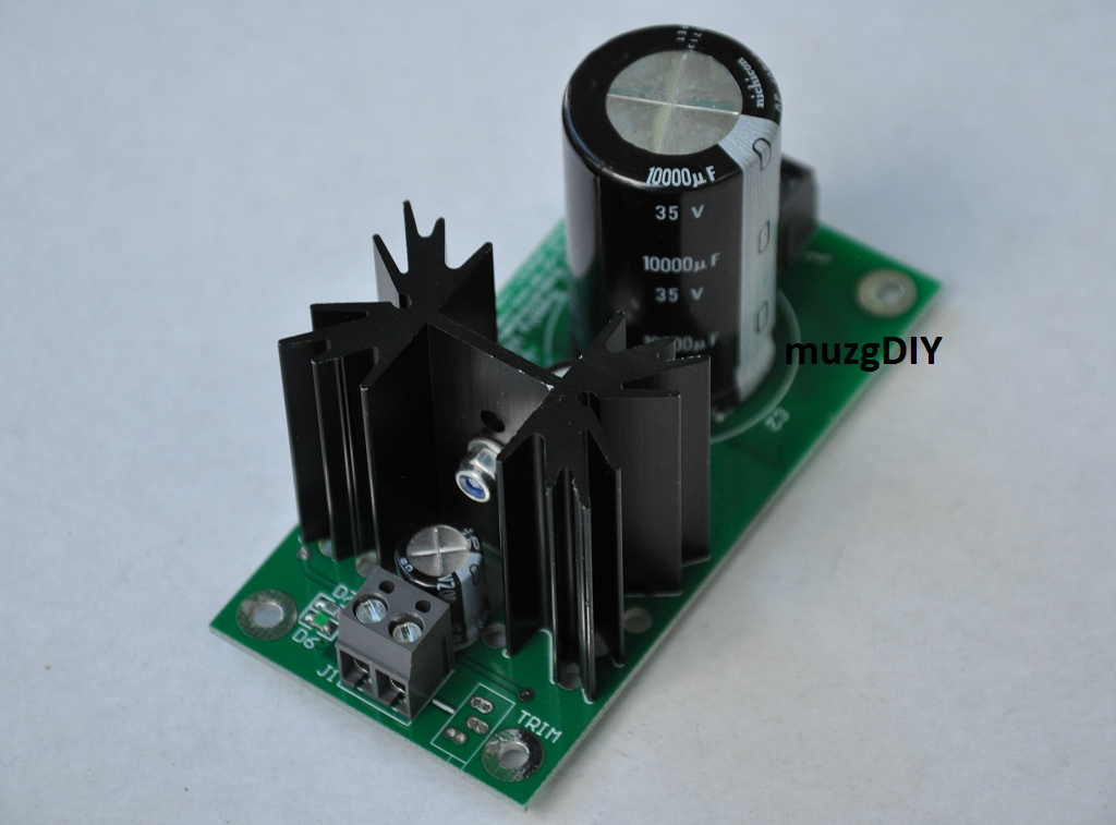
But this is not the end! At the input, after rectifier and smoothing capacitor there is LC pi filter based on Common Mode inductor. Such filter could help to block disturbances which are coming from mains and passes transformer. It is also working in opposite way and blocks disturbances from supplied circuit and not allow them to pass to the transformer.
The PCB of this power supply was created in such a way that helps to remove heat from heatsink. Beneath it there are many holes which in shortest way cool it down.
Dimensions: 45 x 90 mm, high 50 mm
Today I would like to show simple project which I had designed for my friend. My friend has got precision OCXO oscillator taken from old GSM BTS. Device was reworked to support audio frequency 24.576000MHz but at its 50R output it had +3dB sine wave.
Such signal is not sufficient to drive audio chips directly, so some converter was needed. I decided to add the same circuit which I had on the output of my audio clocks.
Tiny PCB contains whole circuit needed to convert signal from +3dB sine wave to CMOS compatible square wave and also its own voltage regulator. Input as well as output impedance is 50R.
Input impedance: 50R
Input coupling: AC
Input signal shape: any
Output impedance: 50R
Output signal shape: square wave
Output amplitude: 3,3 or 5V depends on used regulator
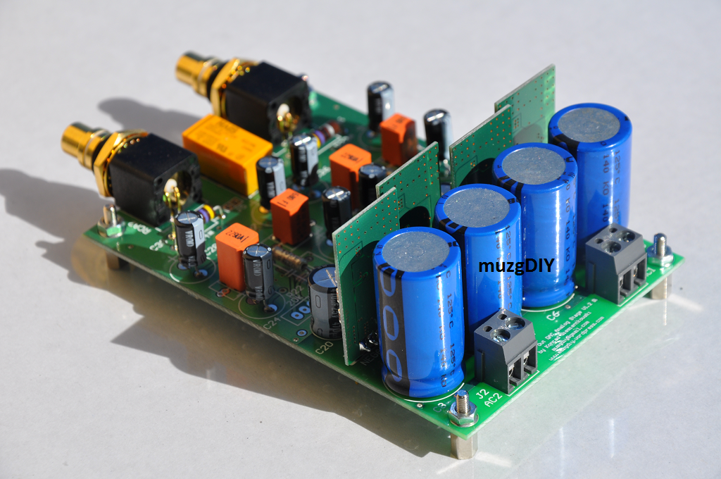
Today I would like to present analog stage for current output DACs which I have been using with PCM63 and PCM1704.
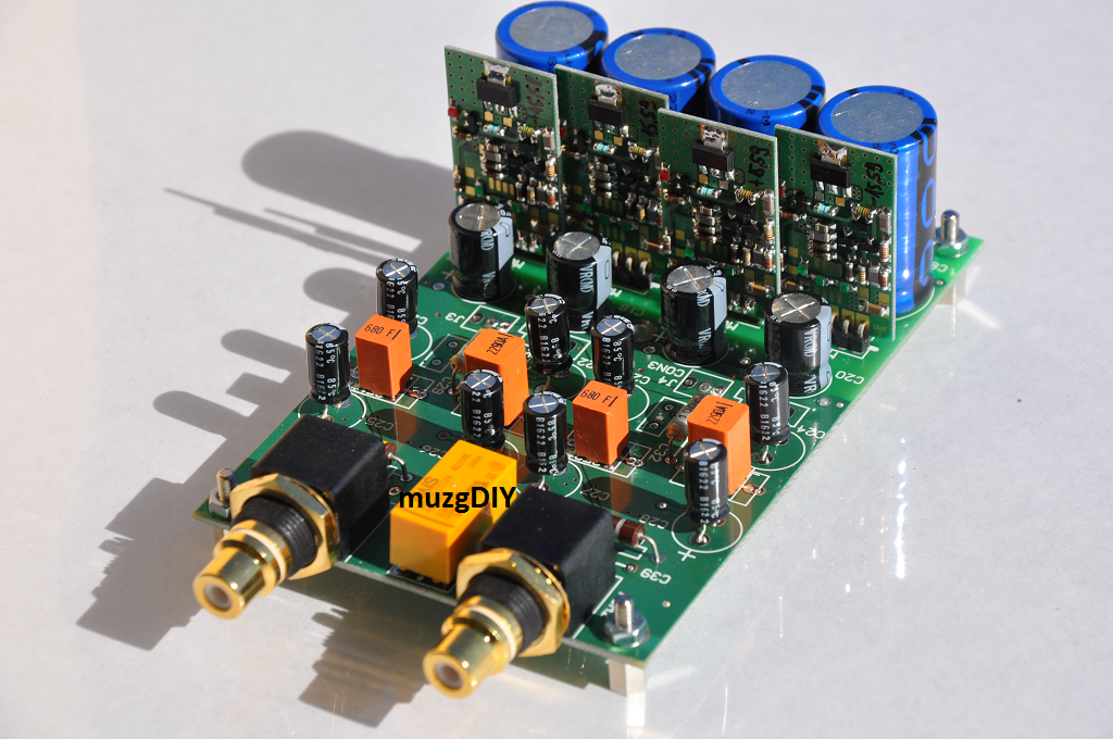
Single PCB consists of complete, ready to use solution. Board to operate requires only transformer. Input of the board should be connected directly to DAC chips.
Following circuits are located on PCB:
– power supply with dedicated for each channel, discrete regulators,
– I/V stage based on opamp
– LPF active filter in MFB topology
– relay for muting circuit
– output connectors directly mounted on rear panel
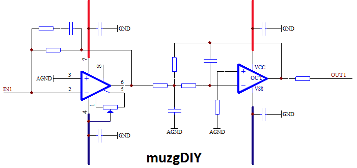
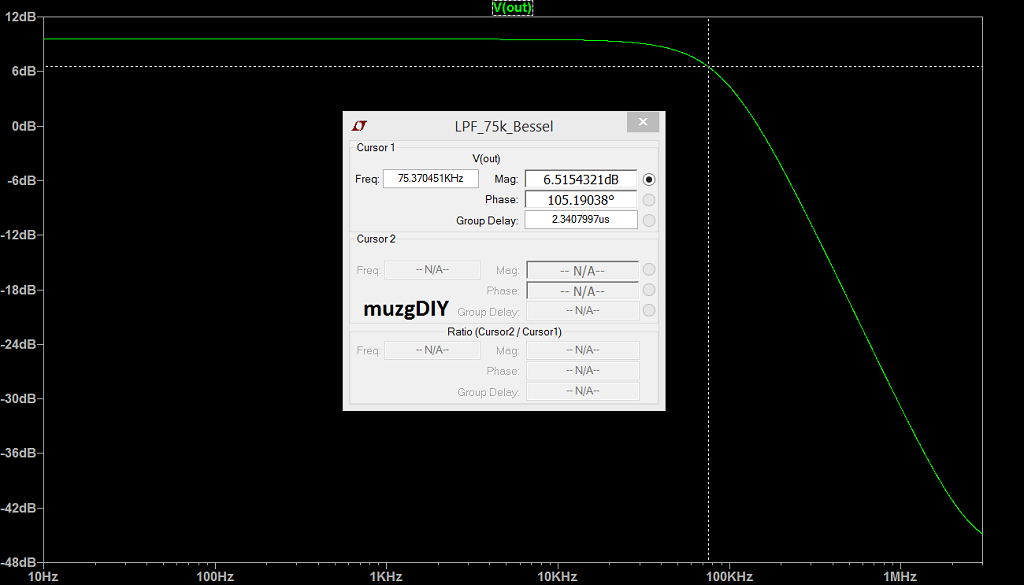
Output active LPF filter is designed in Multiple Feedback topology which is the best for audio applications. Cutoff frequency is set to 75kHz. It means that this analog stage is ideal for DACs with 8x oversampling (44.1kHz) or for sampling rates 352.8kHz.
Opamps used on the board are the best in their class for such applications. I/V stage consists AD797 which is bipolar, high speed, low noise operational amplifier ideal to use in I/V stage. On active filter, due to its capacitive load tolerance and little warm sound, AD825 is used.
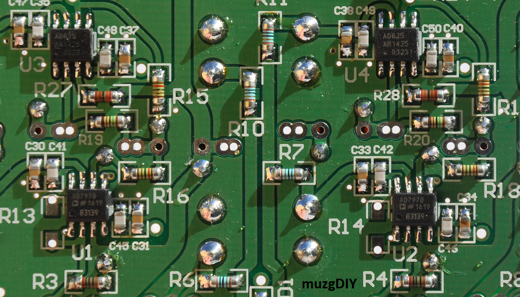
Not only opamps used in this board are hi-end. Each component used on this board is best in its class:
– polystyrene capacitors in filter and compensation circuits,
– COG capacitors in decoupling of opamps,
– Caddock’s resistors in I/V converter – optional!,
– minimelf resistors in filter circuit,
– discrete V3.0max regulators separated for each channel,
– hi-end RCA connectors,
– lot of space for good electrolytic capacitors – nichicon VR as a standard.
This configuration means that sound signature of this board is very dynamic, neutral and velvet. It was confirmed during listening tests and is the best sounding for me (subjectively).
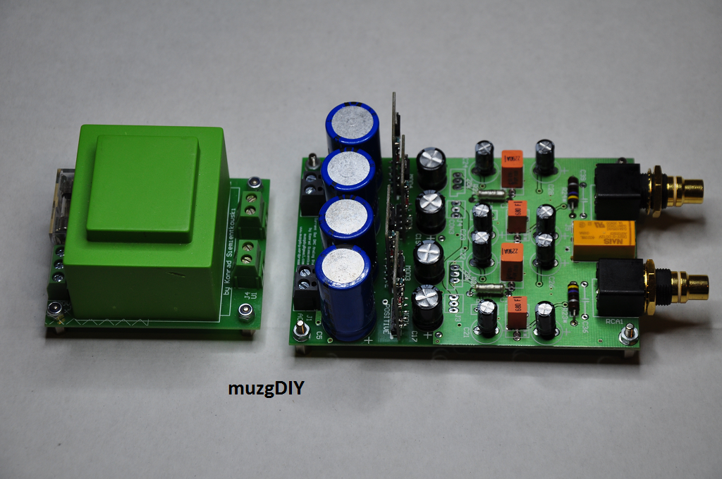
Analog stage can be powered directly from my TEZ transformer board:
Last time I presented integrated solution for heavy power supply, but one integrated solution is enough for some time. Now it’s time for something, as usual – discrete.
Let me show you my precious! Long awaited power supply for applications like:
The main reason to design and build it, was that I want to replace switching power supply for my small PC where my Daphile music server is installed.
Thanks to the complexity of design, board can be configurated as positive or negative regulator. Please, have a look at this board, isn’t it pretty?
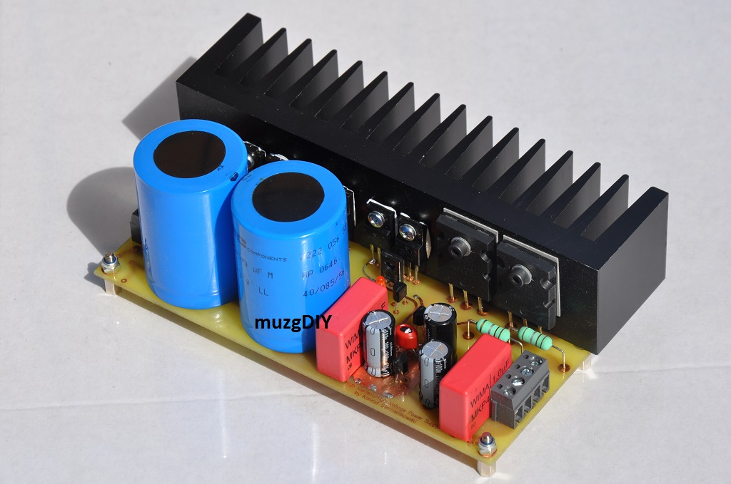
Maximal output current is: 10A
Maximal input voltage: 100V
Higher ratings of current and voltage are possible but have not been tested yet. Maximal values can be achieved interchangeably. It is not possible to build 10A 100V power supply, but f.e.
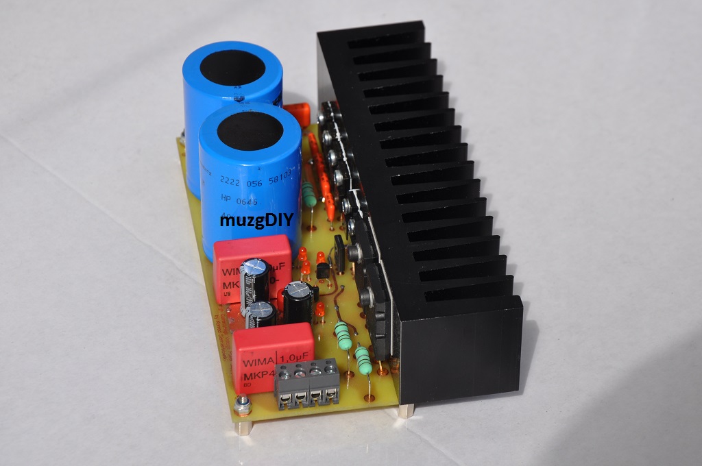
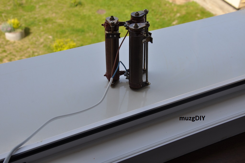
During the test, 120W of heat was dissipated on my dummy load so I decide to put it outside the window.
Next design that i want to publish today is V2.1. This design is based on old V2.0 regulator but simple NPN transistor is used as output device instead of Sziklai pair. Design is quite similar to popular regulators like: ALWSR, TT Feeder, Walt Jung low noise regulator.

V2.1 is constant current source biased series regulator. It is closed loop design with error amplifier built of operational amplifier. Operational amplifier provide accurate regulation in wide temperature range, big open loop amplification and fast transient response.
Voltage reference is made in 2 different ways. One is classic in all of my design – simple LED with low noise. Second is based on precision voltage reference to take a advantage of precision operational amplifier. This creates accurate regulator with low temperature drift. 
V2.1 regulator is one of the best choice to power precision, low noise and fast switching devices like DACs, ADC, digital filters, S/PDIF receivers.
Output voltage can be set between 3,3 – 5V with standard version. Higher voltages requires to use different operational amplifier. Dropout voltage is at least 1,5V, but I recomend values from 2V to 3V. You must calculate this for power dissipation max. 1W. Maximal output current is 500mA, but for provide good stability I recommend max. 200mA (with precision voltage reference could be more).
Welcome after a long break from writing!
Today I would like to show You one of my oldest design of series voltage regulator. V1.2 is exactly V1.0 with greater reference voltage and lot of space for output capacitor. It is also produced on gold plated PCB’s.

V1.2 is constant current sourced biased regulator. It is closed loop device with error amplifier based on single transistor. Voltage reference is done by 2 LEDs. Only transistor/diode design allows to make positive and negative versions of this regulator.
This design is mostly used by my to supply analog circuits with voltages +/-12V and +/-15V. It is also good choice as voltage pre-regulator before accurate and fast V3.1 and V2.1 designs. I use it as output regulator of clock power supply:

Today I would like to show You my strongest from single power supply board. It is based on TEZ16 transformer, Schottky bridge with 3A diodes and V3.1 regulator with high bias current:


Maximal output current: 1100mA @5V (@225Vac)
After 1hour operating with 1100mA (5V) at 27 Celsius degree of ambient temp, heat sink temperature rises 57 Celsius degree.
