Hybrid tube preamplifier is module containing SRPP tube voltage stage and CCS biased source follower based on high voltage MOSFET transistor. CCS is fully discrete bipolar. Both transistors are placed on powerful heatsink.
First stage is the same as in both my fully tube preamplifiers (with cathode follower and White cathode follower) but only difference is that here expensive 6N30P tubes are replaced by more modern components like transistors.
Most of components are SMD type. Only few bigest components are THT. Tubes are mounted on bottom side of PCB to helps
Parameters:
Frequency response: 2Hz – 1.35MHz to 47k load (2.2uF output capacitor
Amplification factor: base 10V/V (20dB
Anode supply: 300V 60mA
Heater supply: 6,3V 700mA
Output impedance: ~100R
Board dimensions: 100 x 100mm
Additional features:
input resistor divider for gain reduction to desired one
place for bypass capacitor on cathode resistor of SRPP circuit to increase gain
muting relay at the output (required external control circuit)
possibility to change heater style from ECC88 like tubes to ECC82 like tubes
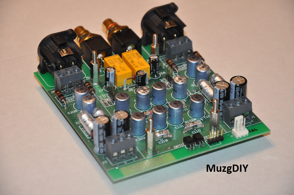
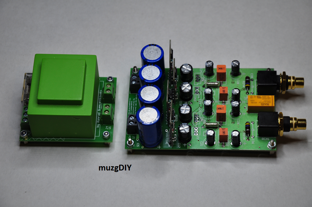
This power supply is complete solution for tube pre- and amplifiers – simple and complex as well. It is based on semiconductors and contains both: anode and heater stabilised power supply.
Maybe you will be surprised, but most of this unit is made of SMD components. Only some critical parts are THT – power, and capacitors.
Circuit is designed to meet even most extreme requirements. Could be used to power simple single tube preamplifier and extreme balanced tube preamplifier with differential amplifier and 4x White Cathode followers created with 6N30P tubes. In addition, it is possible to power small amplifiers for example: stereo EL84 SE Amp, or single channel EL84 PP Amp.
Single PCB contains:
Anode high voltage, regulated power supply 150-350V 200mA with delayed on,
Heater regulated power supply 1,2-12,6V 5A with slow ramp,
Mute delay circuit to control audio output relay – enable output of preamplifier few second after anode supply is activated
Anode power supply is built over discrete high voltage regulator similar to my V3.1 regulators. This means that this regulator is completely discrete, based upon SMD components, specially selected to operate with voltages up to 400V. Output voltage is set by potentiometer or could be set by fixed resistor.
Anode regulator is preceded by CRC smoothing filter for best noise performance and also to increase overall PSRR.
Heater power supply is based on integrated LDO and is capable to deliver up to 5A. Voltage at its output rises slowly from 1,2V to desired voltage in 10s to protect tube heaters from current surge when they are cool. Output voltage selection can be done in 2 ways:
by jumper in predefined steps: 6,3V; 7V; 12,6V
by variable potentiometer in range 1,2 – 13V (could be more)
Bridge rectifier in this circuit is created from 10A Schottky diodes to provide low voltage drop at the input. All this circuit is preceded with CLC smoothing circuit for best noise performance.
Heater supplying voltage is balanced and elevated comparing to anode supply GND by 1/4 of anode voltage. This feature is helpful in circuit when cathodes of tubes are biased by high voltage for example: SRPP, White Cathode Followers, Mu Followers.
The last part of the board is control unit. This circuit contains two part: anode delay circuit and audio muting circuit. Timing is set to 30s delay of anode voltage and 40s for audio mute. Timers as well as relay output are powered by third, 5V regulator. Thanks to this initial delay it is stable in every condition and relay is always powered from stable voltage.
Best thermal performance is achieved by good thermal design. This supply is able to dissipate a lot of power.
And in addition all this things were achieved in dimensions: 100 x 100 x 50mm!!
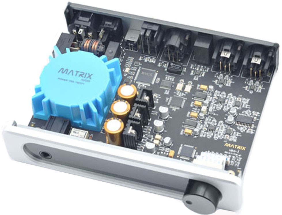
Recently, I was asked to repair Matrix Mini-I Pro. It was death. Mute. I quickly found the cause. It was quite easy defect – few electrolytic capacitors were shorted so I replace them all. I gave DAC the second life. Here you can find how looks Matrix Mini-I Pro DAC when cames from factory (official photo):
Meanwhile, the owner of Matrix come up with the idea to upgrade it. I agreed as I got means to do such improvements. So, DAC was given the second and much better life. I decide to do few modifications using as much as possible of original circuit:
Few better passive components in analog circuit
Of course my best discrete regulators in most sensitive places
Better operational amplifiers in analog circuit
Possible to do, but postponed to second level of modifications:
all resistors to minimelf – circuit is designed to use 0805 resistors, but original pads are able to handle 1206-long resistors
all regulators to discrete MuzgDIY types
replace clock generators to MuzgDIY ones or if this couldn’t be done because of space at least Crystek CCHD
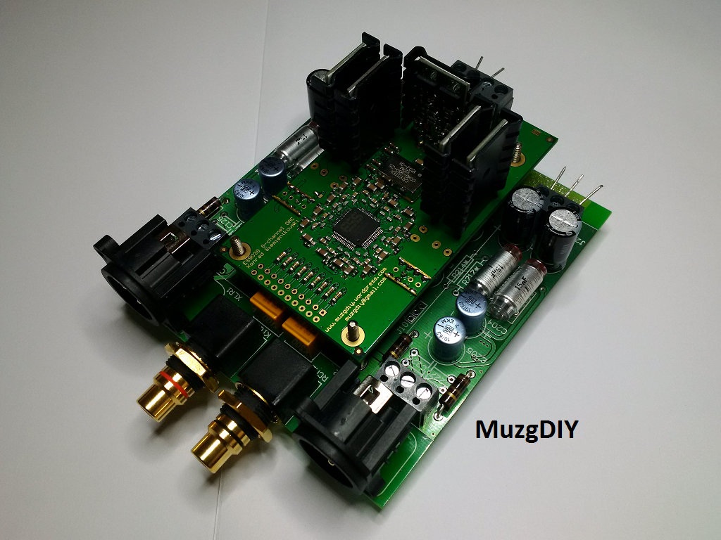
I start a topic concerning my new project that is DAC based on PCM1794A chips. On chips because it may be built either on two or one PCM1794 chip what is configurated by appropiate set of elements (more details on schematic).
As a S/PDIF receiver and I2S switch I used relatively not well known DIX9211 chip. Its main advantages are twelve S/PDIF inputs, support for all formats ranging till 192kHz, a possibility of connecting to three additional 12S signal sources (it may also allow DSD format) and controlling via I2C. DAC also has a space for amanero module with its own power supply and galvanic isolation ISO7640.
Module’s inputs are:
USB via amanero or similar
2x Coax
Toslink
AES/EBU
inner iput I2S e.g. for bluetooth module
DAC is controlled by microcontroller STM32F100RBT6B. STM32F100RBT6B has big amount of periphery that allow to expanse DAC, a lot of GPIO and 128kB of flash memory and that all is well-priced. Additional simplification which is Cube makes there is no other choice. Encoder was planned to be responsible for controlling. Active input indication via separate PCB with OLED on SPI display or 8 LEDs on 74HC595. There is possibility to control via remote control or UART. Updates are made via UART. To PCB programming ST-Link V2 is needed. It is available on each Discovery STM32 module.
Power supplying is extended. I divide it on three sections, each supplied from separate transformer winding.
Post- regulators may be chosen between LT1763 and discrete module. Additionally, I put LC filters in digital sections. Thanks to that they are better separated. Digital module contain 10 voltage regulators. In MONO mode (one PCM1794 for canal?) there is possibility to supply the chip from different regulators (4pcs,) or mounting jumper and using only two – one for digital and one for analogue.
The whole construction I divide on two different modules – digital PCB with DAC chips (150x120mm) and totally symmetrical analogue module with the same dimensions (not ready yet). Such division make it elegant and not as big as a computer board, and what matters more it leave a space to experiment with other analogue variants, also with lamps.
I plan to build analogue module as follow:
I/V converters on single opAmps SMD AD797 or OPA1611 type
symmetrical filter based on MFB on OPA1632 configuration
power supply either LT1963/3015 or discreet modules, two per each canal
mute for noise elimination
without capacitors in signal path
Later I will work out lamp module.
The whole circuit, where it possible, in SMD. The elements dimensions from 0603 to 1210. PCB is still being worked out. I attach the look/view.
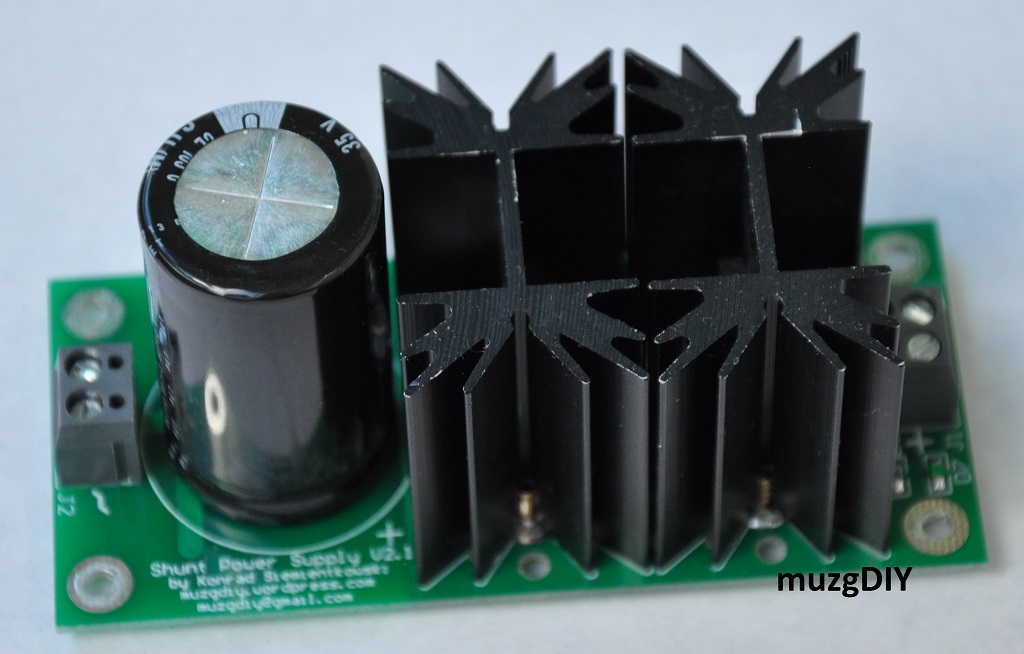
Shunt power supplies always are not so simple in use as series but all shunt fans knows, that this effort will pay of. And for that people’s I have got something special. New power supply with high current capability. Input CCS can be set up to 1000mA!
For everyone who would like to say that it is Salas I want to say: you are wrong! It is my proprietary, bipolar design, similar to V8.0 regulator and taking best from both – V3.1 and V8.0 regulators.
Designed in the way that can be used instead of popular „S” power supplies or even replace it in ready designs. Comparing to its famous competitor:
– requires less voltage drop across regulator – typically 1,5V
– is more flexible – from few up to 1000mA BIAS current
– output voltage can be set from 3 to 15V by fixed resistor or helipot.
– very stable output voltage during warming – no more worry about your circuit!
– stable output voltage in function of output current – no more worry about your circuit!
– CLC input filter to block noise in both ways
From user experience I can guarantee that performance and sound is similar or even better.
Board presented below is my own implementation of opamp analog stage for best sounding DACs in the world. Privately I am big fan of Sabre32 chips, especially S and PRO series and I did this board to take the best from of them.
Board is designed to hold digital section under its components. Place for digital board is compatible with my Sabre S and PRO boards and Buffalo ones.
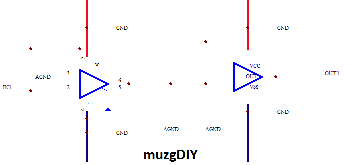
As usual in my projects, I/V Stage uses AD797 (4pcs) opamp which is the best sounding chip for this application. Filtering of output signal is passive like on ESS recommended design. Fully differential output circuit utilizes OPA1632 (2pcs) . Every power supply pin is decoupled with 3 capacitors and connected via their own resistor to supply lines.
Board could be powered in dual mono mode by 2pcs. of +/-15V power supply or by only one in stereo mode. This feature is chosen by placing jumpers on bottom side of PCB.
Board contains very sophisticated muting circuit with:
delay during turn on
fast detection of turning off by falling slope on supply voltage
galvanically isolated connection to ES9018S status pins to detect whether chip is muted or unlocked.
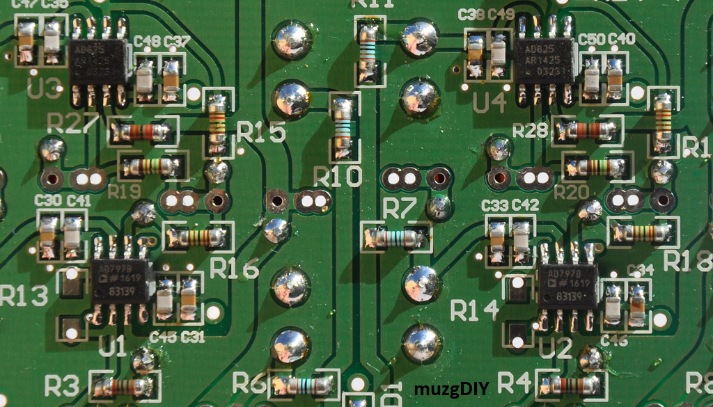
Today I would like to present analog stage for current output DACs which I have been using with PCM63 and PCM1704.
Single PCB consists of complete, ready to use solution. Board to operate requires only transformer. Input of the board should be connected directly to DAC chips.
Following circuits are located on PCB:
– power supply with dedicated for each channel, discrete regulators,
– I/V stage based on opamp
– LPF active filter in MFB topology
– relay for muting circuit
– output connectors directly mounted on rear panel
Output active LPF filter is designed in Multiple Feedback topology which is the best for audio applications. Cutoff frequency is set to 75kHz. It means that this analog stage is ideal for DACs with 8x oversampling (44.1kHz) or for sampling rates 352.8kHz.
Opamps used on the board are the best in their class for such applications. I/V stage consists AD797 which is bipolar, high speed, low noise operational amplifier ideal to use in I/V stage. On active filter, due to its capacitive load tolerance and little warm sound, AD825 is used.
Not only opamps used in this board are hi-end. Each component used on this board is best in its class: – polystyrene capacitors in filter and compensation circuits, – COG capacitors in decoupling of opamps, – Caddock’s resistors in I/V converter – optional!, – minimelf resistors in filter circuit, – discrete V3.0max regulators separated for each channel, – hi-end RCA connectors, – lot of space for good electrolytic capacitors – nichicon VR as a standard.
This configuration means that sound signature of this board is very dynamic, neutral and velvet. It was confirmed during listening tests and is the best sounding for me (subjectively).