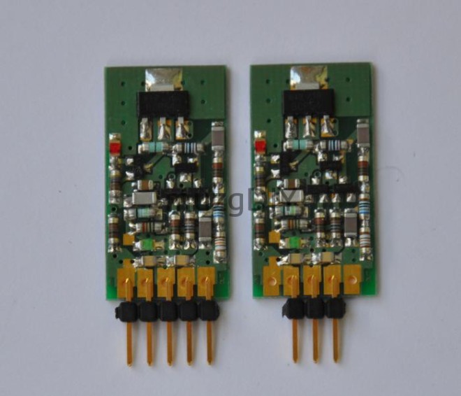
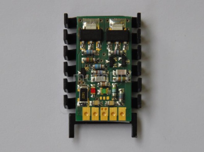
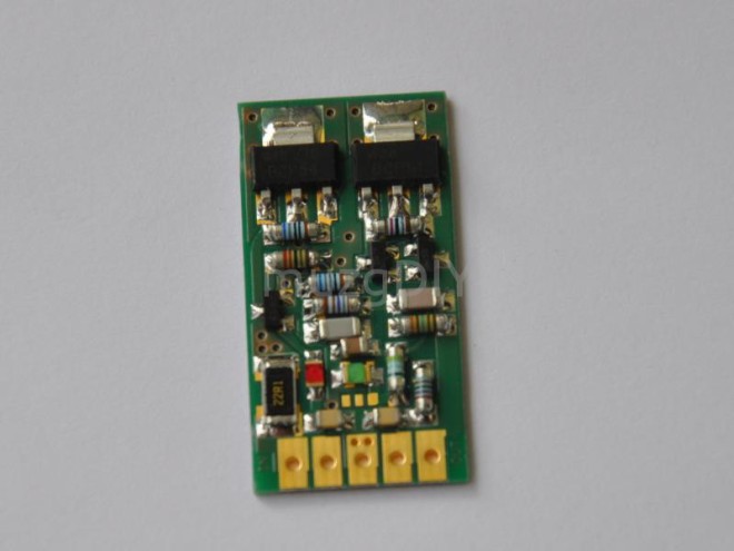
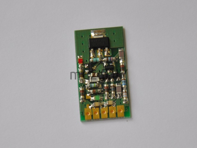
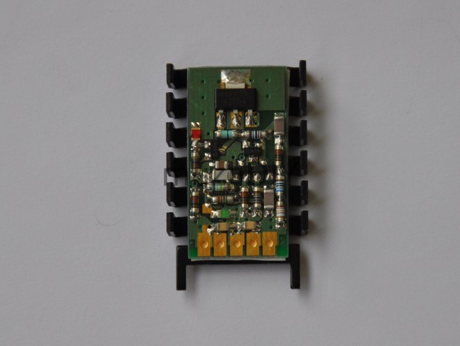
New in Family – V9.0 Shunt Regulator

After long break from designing new voltage regulator topologies I decided to create some shunt regulator with opamp based error amplifier.

Like all my shunt regulator this one is also uses Shiklai based current source at the input but rest of design is totally different but it is nothing new on the market. Similar topology is used in TPA Trident regulator and Tent Regulator but it not has a disadvantages of the first one. Output voltages not varies from input voltage and is stable in every load condition.

Current can be set up to 100mA!

Specially designed to power precision audio components like: DACs, ADCs, S/PDIF receivers, clock circuits.

Voltage reference based on LED diode to ensure low noise. There are possibility to use precision voltage reference instead of LED diode for good voltage precision and temperature stability.

Simply decoupling circuit on regulator PCB is sufficient to ensure stability of regulator but external high capacity can be connected to provide low ripple with high speed output current change.

Dropout voltage is at least 1,5V, but I recomend values from 2V to 3V. You must calculate this for power dissipation max. 1W.

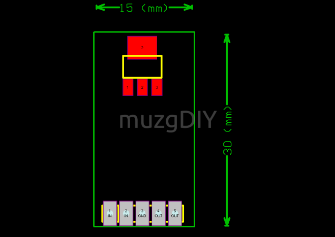
Pinout compatible with standard LM78XX regulators like LM7805 and similar. If LM78XX regulator will be replaced by V8.0 only 3 central pins can be used. If board is developed specially for V8.0 all 5 pin can be used.

Dimensions are always the same: 30mm x 15mm.

Precise and Fast – V2.1 series regulator

Next design that i want to publish today is V2.1. This design is based on old V2.0 regulator but simple NPN transistor is used as output device instead of Sziklai pair. Design is quite similar to popular regulators like: ALWSR, TT Feeder, Walt Jung low noise regulator.

V21_front_LED

V2.1 is constant current source biased series regulator. It is closed loop design with error amplifier built of operational amplifier. Operational amplifier provide accurate regulation in wide temperature range, big open loop amplification and fast transient response.

Voltage reference is made in 2 different ways. One is classic in all of my design – simple LED with low noise. Second is based on precision voltage reference to take a advantage of precision operational amplifier. This creates accurate regulator with low temperature drift. V21_front_Precision

V2.1 regulator is one of the best choice to power precision, low noise and fast switching devices like DACs, ADC, digital filters, S/PDIF receivers.

Output voltage can be set between 3,3 – 5V with standard version. Higher voltages requires to use different operational amplifier. Dropout voltage is at least 1,5V, but I recomend values from 2V to 3V. You must calculate this for power dissipation max. 1W. Maximal output current is 500mA, but for provide good stability I recommend max. 200mA (with precision voltage reference could be more).

Simple but Flexible – V1.2 series regulator

Welcome after a long break from writing!

Today I would like to show You one of my oldest design of series voltage regulator. V1.2 is exactly V1.0 with greater reference voltage and lot of space for output capacitor. It is also produced on gold plated PCB’s.

V12_front_1

V1.2 is constant current sourced biased regulator. It is closed loop device with error amplifier based on single transistor. Voltage reference is done by 2 LEDs. Only transistor/diode design allows to make positive and negative versions of this regulator.

This design is mostly used by my to supply analog circuits with voltages +/-12V and +/-15V. It is also good choice as voltage pre-regulator before accurate and fast V3.1 and V2.1 designs. I use it as output regulator of clock power supply:

Clock_supply_1_1

Discrete Bipolar Power Supply V1.2

Today I would like to show You one of my bipolar power supplies. It is based on same topology like in V3.X series but with cascade bias constant current source and with CCS in Vref. Discrete_1

Discrete_2

Board are very compact. Only few largest component are located at top side of PCB – rest are in SMD on bottom side.

Discrete_3

Shape of the board, dimensions and mounting holes positions are the same like in rest of my bipolar power supplies so can be swapped for choosing the best for us.

Dimensions of PCB: 60 x 82mm

Integrated constant current sources and voltage reference  circuit consist 12 LED’s so board emits light also. Output voltage is set by feedback voltage divider mounted on board – should be set during assembling.

To use this power supply You must provide only 2 x AC voltage to connectors one one edge of PCB. Here You can find example of use with my transformer board:

Discrete_4

Maximal output Current: 500mA @15V

Maximal Power dissipation: 2W/channel

16W Power Supply

Today I would like to show You my strongest from single power supply board. It is based on TEZ16 transformer, Schottky bridge with 3A diodes and V3.1 regulator with high bias current:

16W_Supply_2

16W_Supply_1

16W_Supply_3

Maximal output current: 1100mA @5V (@225Vac)

After 1hour operating with 1100mA (5V) at 27 Celsius degree of ambient temp, heat sink temperature rises 57 Celsius degree.

VX.X – Voltage Regulators versions explanation

Till today (24 April 2015) I have designed 14 versions of voltage regulators of which as many as 9 are newly and my own topologies. I know You could have a problem to choose a right one for Your application, so I would like to explain You differences between all versions.

All_3pin

In general there are 3 groups.

  •  discrete series regulators
  •  discrete shunt regulators
  •  integrated regulators (series)

In explanation:

  • V1.0 – simple series regulator with NPN output, single transistor error amplifier, LED voltage reference and CSS bias    circuit.

  • V1.1 – simple series regulator with Szikai output, single transistor error amplifier, LED voltage reference and CSS bias circuit.

  • V1.2 – V1.0 with some improvement for high output voltage, gold plated PCBs.

  • V2.0 – series regulator with opamp error amplifier, Szikai output, LED voltage reference and CCS bias circuit.

  • V2.1 – series regulator with opamp error amplifier, NPN output, LED voltage reference and CCS bias circuit, gold plated PCBs.

  • V3.0 – series regulator with transistor differential amplifier, NPN output, LED voltage reference, CCS bias circuit.

  • V3.1 – V3.0 with some improvements for better soldering, precision voltage reference, precision output voltage set, gold plated PCBs.

  • V3.0max – V3.0 with improvements for high output voltage, gold plated PCBs.

  • V4.0 – shunt regulator based on TL431 with Sziklai CCS, gold plated PCBs.

  • V5.0 – series regulator with opamp error amplifier in shunt configuraton, gold plated PCBs.

  • V6.1 – series regulator based on Texas Instruments TPS7A4700/3301, gold plated PCBs.

  • V8.0 – shunt regulator with transistor differential amplifier, Sziklai CCS, precision/LED voltage reference, gold plated PCBs.

All deigns (excluding V3.0max) are made on 30mm x 15mm PCBs like this:

V3X_35pin_1

Pinout always are:

  1.  IN
  2.  IN
  3.  GND
  4.  OUT
  5.  OUT

so they can replace integrated regulators like 78XX or discrete like TPA Trident Shunt.

You can use only 3 center pins for replacement of 78XX, or all 5 pins when board is designed to use my discrete regulators.

For better heat dissipation external heatsink can be used. I use Fisher heatsinks mounted by 3M heat-conductive tape:

V8_heatsink_1

This tape can be also used to stick the regulator to any metal elements of Your device. Here You can find V1.0 regulators mounted on Revox B226 CD to provide better opamp supply:

V1_heatsink_3

For detailed information about specific version please choose right one from menu. Not all version are carefully described on my page.

Hot and naked – V8.0 discrete Shunt Regulator

Today I have something for Shunt Regulator fans – V8.0 Shunt Regulator!

V8_overview_1

Based on V3.X error amplifier design, with LED biased, Sziklai Constant Current Source.

Current can be set up to 100mA!

I recommend to use it with dedicated heatsink because Shunt Regulators always dissipate power.

V8_heatsink_1

Specially designed to power precision audio components like: DACs, ADCs, S/PDIF receivers, clock circuits.

Output voltage can be set by components in negative feedback circuit from 1V2 to 9V eg. : 1V2, 2V5, 3V3, 5V, 6V, 8V, 9V. Transistor circuit allows to build version for negative voltage.

Voltage reference based on LED diode to ensure low noise. There are possibility to use precision voltage reference instead of LED diode for good voltage precision and temperature stability.

Simply decoupling circuit on regulator PCB is sufficient to ensure stability of regulator but external high capacity can be connected to provide low ripple with high speed output current change.

Dropout voltage is at least 1,5V, but I recomend values from 2V to 3V. You must calculate this for power dissipation max. 1W.

Pinout compatible with standard LM78XX regulators like LM7805 and similar. If LM78XX regulator will be replaced by V8.0 only 3 central pins can be used. If board is developed specially for V8.0 all 5 pin can be used.

Dimensions are always the same: 30mm x 15mm.

Small but Complex – V3.X series regulator

Welcome in my first post!

I would like to show you my lovely child – V3.X series voltage regulator based on discrete components.

V3X_overview_1

Specially designed to power precision audio components like: DACs, ADCs, S/PDIF receivers, clock circuits.

Output voltage can be set by components in negative feedback circuit from 1V2 to 9V eg. : 1V2, 2V5, 3V3, 5V, 6V, 8V, 9V. For higher output levels I recommend V3.0max version. Transistor circuit allows to build version for negative voltage.

Voltage reference based on LED diode to ensure low noise. There are possibility to use precision voltage reference instead of LED diode for good voltage precision and temperature stability.

Simply decoupling circuit on regulator PCB is sufficient to ensure stability of regulator but external high capacity can be connected to provide low ripple with high speed output current change.

Dropout voltage is at least 1,5V, but I recomend values from 2V to 3V. You must calculate this for power dissipation max. 1W.

Maximal output current is 500mA, but for provide good stability I recommend max. 200mA.

For better power dissipation additional heatsink can be used:

V3X_heatsink_1

Pinout compatible with standard LM78XX regulators like LM7805 and similar. If LM78XX regulator will be replaced by V3.1 only 3 central pins can be used. If board is developed specially for V3.X all 5 pin can be used:

V3X_35pin_1

Pin assignment and dimensions:

V3X_dimensions_1

Overall dimensions: 30 mm x 15mm.

V3.X series are tiny implementation of my design used few years ago to supply analog circuit of PCM63P-K DAC. This implementation is specially developed for Buffalo III DAC to replace Trident regulators.

V3.0 inside my Buffalo III DAC:

Staby_V3_Buffalo_3

Thanks for your attention!

Create a website or blog at WordPress.com

Up ↑