Fully differential input stage for power amplifiers

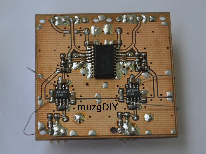
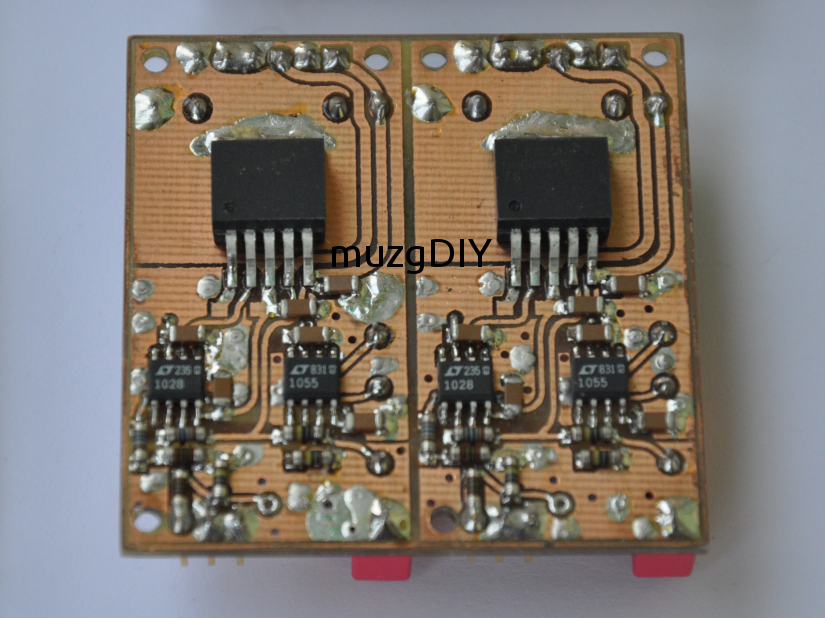
After success with my simple input stage in feeding IcePower Amplifiers with signal I decided to design new, complex input stage with XLR/RCA input and differential output.

Module has fully differential architecture with 2 pcs. of single op-amp at the input and differential amplifier OPA1632 at the output. I’m using DIP8 op-amps at the front to allow user to modify sound to its own preferences. Anyway OPA134 is a good choice for class D users (like IcePower) due to its warm Sound generated by FET input circuit.

Switch between XLR and RCA connector is used to choose right input.

Switch located at the centre of the board is used to select the gain which will be applied to the input signal. Differential gain is selectable between -6dB to 6dB in four steps.

Gain: -6dB to 6dB
Imput impedance: 100kΩ
Output impedance: 50Ω
Frequency response (-3dB): 300kHz limited by RC filter
Power supply: +/-12 – 24V (eg. Directly from IcePower module)
Power cunsumption: 100mA with OPA134
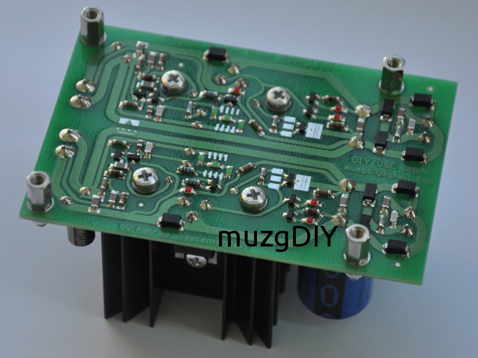
Dimensions: 80 x 60 x 35mm

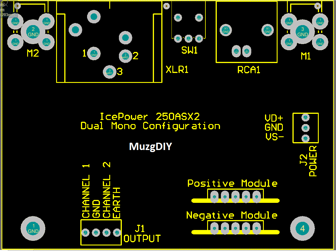
Pinout of the module:

Simple but Flexible – V1.2 series regulator

Welcome after a long break from writing!

Today I would like to show You one of my oldest design of series voltage regulator. V1.2 is exactly V1.0 with greater reference voltage and lot of space for output capacitor. It is also produced on gold plated PCB’s.

V12_front_1

V1.2 is constant current sourced biased regulator. It is closed loop device with error amplifier based on single transistor. Voltage reference is done by 2 LEDs. Only transistor/diode design allows to make positive and negative versions of this regulator.

This design is mostly used by my to supply analog circuits with voltages +/-12V and +/-15V. It is also good choice as voltage pre-regulator before accurate and fast V3.1 and V2.1 designs. I use it as output regulator of clock power supply:

Clock_supply_1_1

Discrete Bipolar Power Supply V1.2

Today I would like to show You one of my bipolar power supplies. It is based on same topology like in V3.X series but with cascade bias constant current source and with CCS in Vref. Discrete_1

Discrete_2

Board are very compact. Only few largest component are located at top side of PCB – rest are in SMD on bottom side.

Discrete_3

Shape of the board, dimensions and mounting holes positions are the same like in rest of my bipolar power supplies so can be swapped for choosing the best for us.

Dimensions of PCB: 60 x 82mm

Integrated constant current sources and voltage reference  circuit consist 12 LED’s so board emits light also. Output voltage is set by feedback voltage divider mounted on board – should be set during assembling.

To use this power supply You must provide only 2 x AC voltage to connectors one one edge of PCB. Here You can find example of use with my transformer board:

Discrete_4

Maximal output Current: 500mA @15V

Maximal Power dissipation: 2W/channel

As small as possible – V2.1 OPAMP

Today I want to show You my precious – V2.1 OPAMP – tiny discrete implementation of single opamp. Pinout is same like in common single opamps on the market so can be used as replacement for many DIP-8 opamps.

Opamp_comparsion_1

Some parameters:

– Supply voltage: max. 36V or +/-18V

– Quiescent current: 20mA

– GBW: TBD

– Slew rate: TBD

– Open Loop Gain: TBD

– Stable with gain from +1 (version with internal compensation)

It is 11 transistor design, fully bipolar, using matched and thermally coupled transistors. Now device is still under development. I’m working on optimisation of open loop gain, compensation. Output offset voltage can be tuned using potentiometer like in LT1028 opamp.

Pinout is also the same like in common amplifiers on the market eg. LT1028:

Pinout

Dimensions of PCB: 11mm x 11mm

I developed two versions of this amplifier. First with internal compensation, stable with gain from +1 and second without compensation – must be done on layout.

Opamp_Front_1

Here is the family of OP AMPs. Left upper one is dual version of my discrete OPAMP, next we can see two singles. At the bottom there are some its integrated cousins which are best in their classes.

Tiny Diamond Buffer Module

Today I would like to show You tiny Diamond Buffer module designed by my friend Krzysztof. Modules are based on topology used by Marantz in HDAM-SA2, but at this time with different components..

Diamond_buffer_SA2

Topology is same like in HDAM-SA2:

All_versions_2

Pinout:

1. VSS
2. VSS
3. OUT
4. IN
5. VCC
6. VCC

Modules are very tinny. Dimensions are 20mm x 20mm.

It can be used as audio buffers or input section of current feedback amplifiers.

Headphone Protection V2.1

Today I would like to show You my protection circuit.

This circuit is designed to do few functions:

– delay at startup – few seconds set by RC

– DC protection

– AC interruption detection for cancelling pops after switching off device.

Circuit are fully discrete and it is my own design. Also circuit has built-in LED indicator.

Output OK:

Prot_OK1

Output Not OK,or during start-up delay:

Prot_NOK1

Dimensions of board: 50mm x 50mm.

TPA6120 + LT1028 for HeadFun

Next amplifier for HeadFun is based on TPA6120 TI current feedback, high current, operational amplifier + Linear LT1028 for input buffer/voltage amplification. TPA6120 needs input buffer on non-inverting input due to ~6uA of current sourcing from this pin.

HeadFun_TPA6120_1

LME49600 + LT1028 for HeadFun

Next headphone amplifier module designed to use witch HeadFun mainboard is based on LME49600/610 TI buffer witch LT1028 voltage amplifier and LT1055 DC servo.

HeadFun_LME49600_1

Electrolytic and DC servo capacitors are mounted at bottom side of PCB. I really like this combination of opamps. LT1028 and AD797 are my favourite opamps for voltage amplification. LT1055 has very good performance in DC servos cause of low input current and low current noise. This combined with big values of resistors at input gives good noise performance.

Feedback loop is voltage type. Voltage amplification is set to 10x.

HDP01 Discrete for HeadFun

Design based on corrected and improved schematic originaly posted by Knut Harald Nygaard on his home page:

http://www.andiha.no/index.html

but now project is unavailable, maybe cause of instability of original design.

Input circuit is pair of JFET (I’m using 2SK246BL/J103BL). Current from input was mirrored in bipolar current mirror, and directly connected to bipolar MOSFET source follower. Circuit is using current feedback loop.

My first implementation of this amplifier is quite big, but sound quality is amazing!

https://picasaweb.google.com/muzg123/CFAHeadampHDP01

My second implementation is module for HeadFun amplifier made from SMD components (excluding electrolytic caps and JFETs) and PCB as heatsink:

HeadFun_HDP01_1

Not only sound quality of HDP01 is incredible. Measurements also shows good result:

THD+N 1kHz -3dB output level (referenced to input level of EMU1616), load 270R:

THD+N

IMD+N with the same conditions:

IMD+N

Results in RMAA:

Wyniki_RMAA

Finally, till now this is the best sounding headphone amplifier that I ever heard! I’m using it with Sennheiser HD580 headphones.

Create a website or blog at WordPress.com

Up ↑