In addition to my „Fully Tube, regulated HV Anode Power Supply” i have created second PCB which is additional regulated power supply to cover heater of powered tubes. Board is exactly half of my „Highly integrated supply for Tube Preamplifiers”, adjusted to control relay.

Created to provide complete solution for powering tube preamplifiers and make it fully regulated.

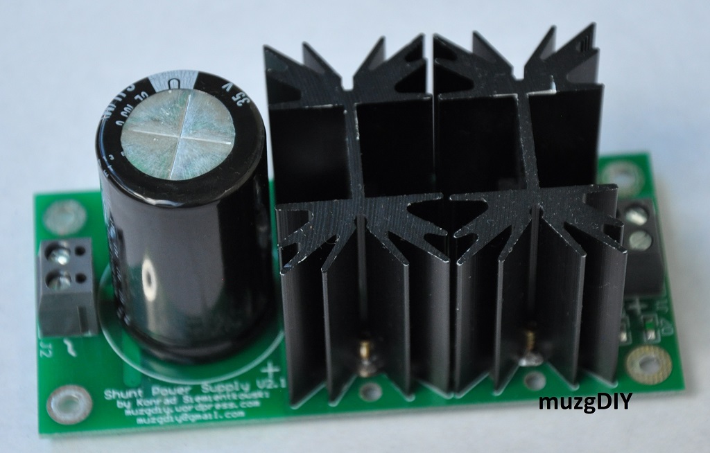
Heater power supply is based on integrated LDO and is capable to deliver up to 5A. Voltage at its output rises slowly from 1,2V to desired voltage in 10s to protect tube heaters from current surge when they are cool. Output voltage selection can be done in 2 ways:
- by jumper in predefined steps: 6,3V; 7V; 12,6V
- by variable potentiometer in range 1,2 – 13V (could be more)

Bridge rectifier in this circuit is created from 10A Schottky diodes to provide low voltage drop at the input. All this circuit is preceded with CLC smoothing circuit for best noise performance.
Heater supplying voltage is balanced and elevated comparing to anode supply GND by 1/4 of anode voltage. This feature is helpful in circuit when cathodes of tubes are biased by high voltage for example: SRPP, White Cathode Followers, Mu Followers.

The last part of the board is control unit. This circuit contains two part: anode delay circuit and audio muting circuit. Timing is set to 30s delay of anode voltage and 40s for audio mute. Timers as well as relay output are powered by third, 5V regulator. Thanks to this initial delay it is stable in every condition and relay is always powered from stable voltage.